We are studying Photonic Integrated Circuits. ▷Japanese
7-1, Kioi-cho, Chiyoda-ku, Tokyo 102-8554
Room 4-275A
Selective MOVPE
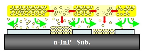
Selective metalorganic vapor phase epitaxy (MOVPE) is one of the most attractive
methods for fabricating integrated multiple quantum well (MQW) optical
waveguide devices. This is because different bandgaps of MQW structures
can be easily realized in a wafer by changing only the dielectric mask
geometry in a single selective MOVPE growth step. In addition, selective
MOVPE in a narrow stripe region enables direct waveguide formation without
a semiconductor etching process. The waveguide structures fabricated by
the direct waveguide formative selective MOVPE process along the [011]
directions on (100) substrates are automatically surrounded by the (100)
and (111)B crystal planes. They have mirror surfaces and the waveguide
dimension can be controlled with photolithographic accuracy of the dielectric
mask patterning so that a well-controlled ideal optical waveguide structure
can be realized. Using the above-mentioned advantages, advanced optical
devices have been reported such as a precisely wavelength controlled laser
diodes, and a low-loss passive optical waveguide. These excellent characteristics
for the advanced waveguide devices are obviously attributed to the highly
controllable and reproducible features of the direct-waveguide-formative
selective MOVPE method.


バナースペース
Shimolab
7-1, Kioi-cho, Chiyoda-ku,
Tokyo 102-8554
Room 4-275A